[DRAFT] Making some PCBs - part 3 (MAX9850)
Stage 2 - MAX9850
2-layer board.
I also got started designing an audio extension board featuring the MAX9850 stereo audio DAC with builtin headphone amplifier.
Now the MAX9850 part comes in TQFN-28 which is an absolutely tiny package with 0.5mm pitch (the KiCad footprint is “TQFN-28-1EP_5x5mm_P0.5mm_EP3.25x3.25mm”). See comparison below to get an idea how tiny this really is.
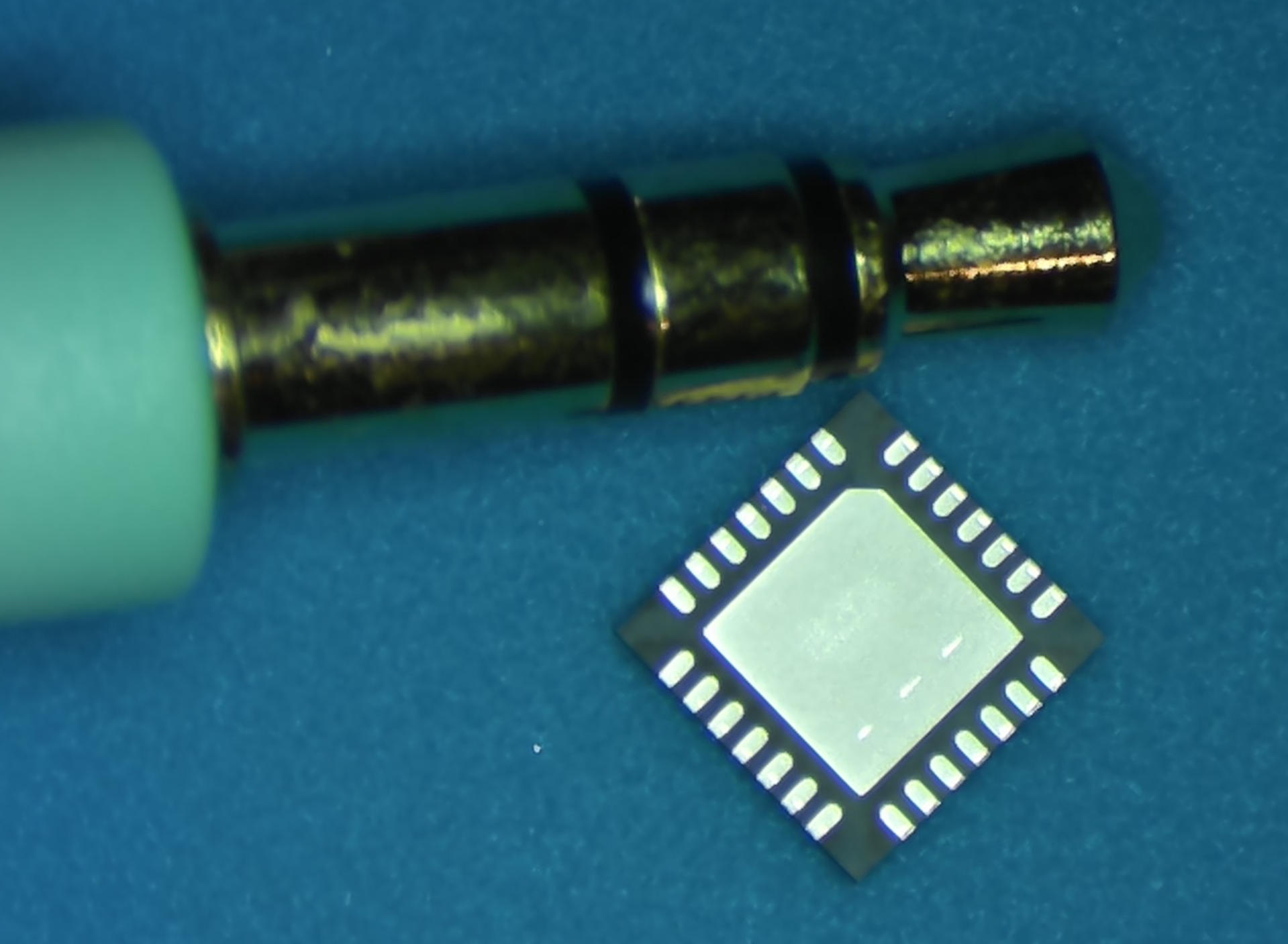 MAX9850 next to a standard 3.5mm audio plug.
PCB design
Using the best of my currently rather amateurish PCB design skills I ended up with the following layout with KiCad project files on GitHub.
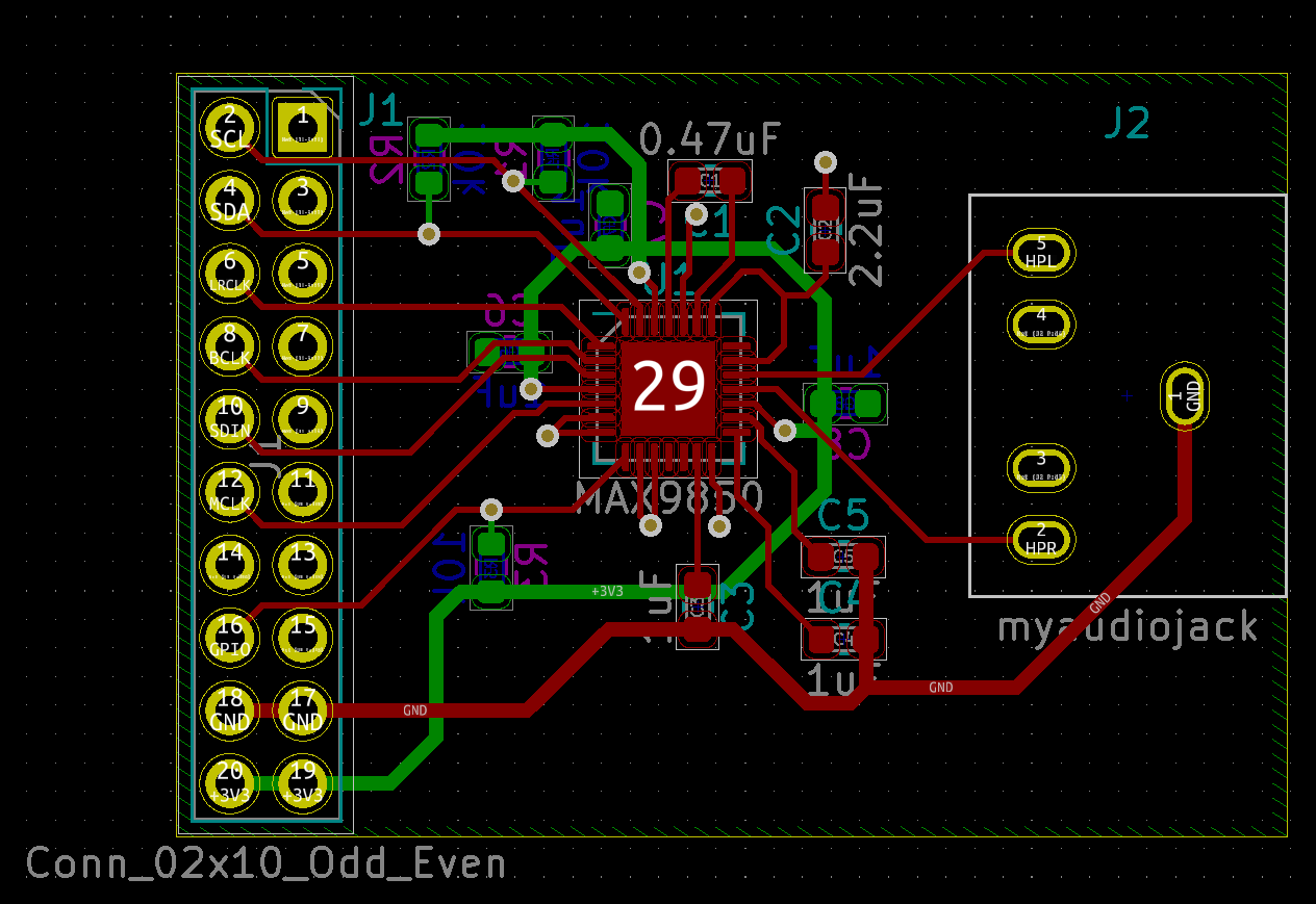
While it initially looked pretty good to me I realize that is has a number of layout flaws that I will need to remedy before I attempt the combined ECP5 board. To this end I have signed up for the Mixed-Signal Hardware Design with KiCad course from well known YouTube creator Phil’s Lab. Having browsed through the 5 hour video material that focuses heavily on PCB layout I can only say that this appears to be a goldmine. So after finishing this board I will probably take a detour to study the course material and follow along with its board project.
Assembly
Again soldering the top side using stencil and paste. The board is placed on a hot-plate that slowly rises to 220C after which hot air is applied from above for about 20-30s with station set to 300C at 30l/min.
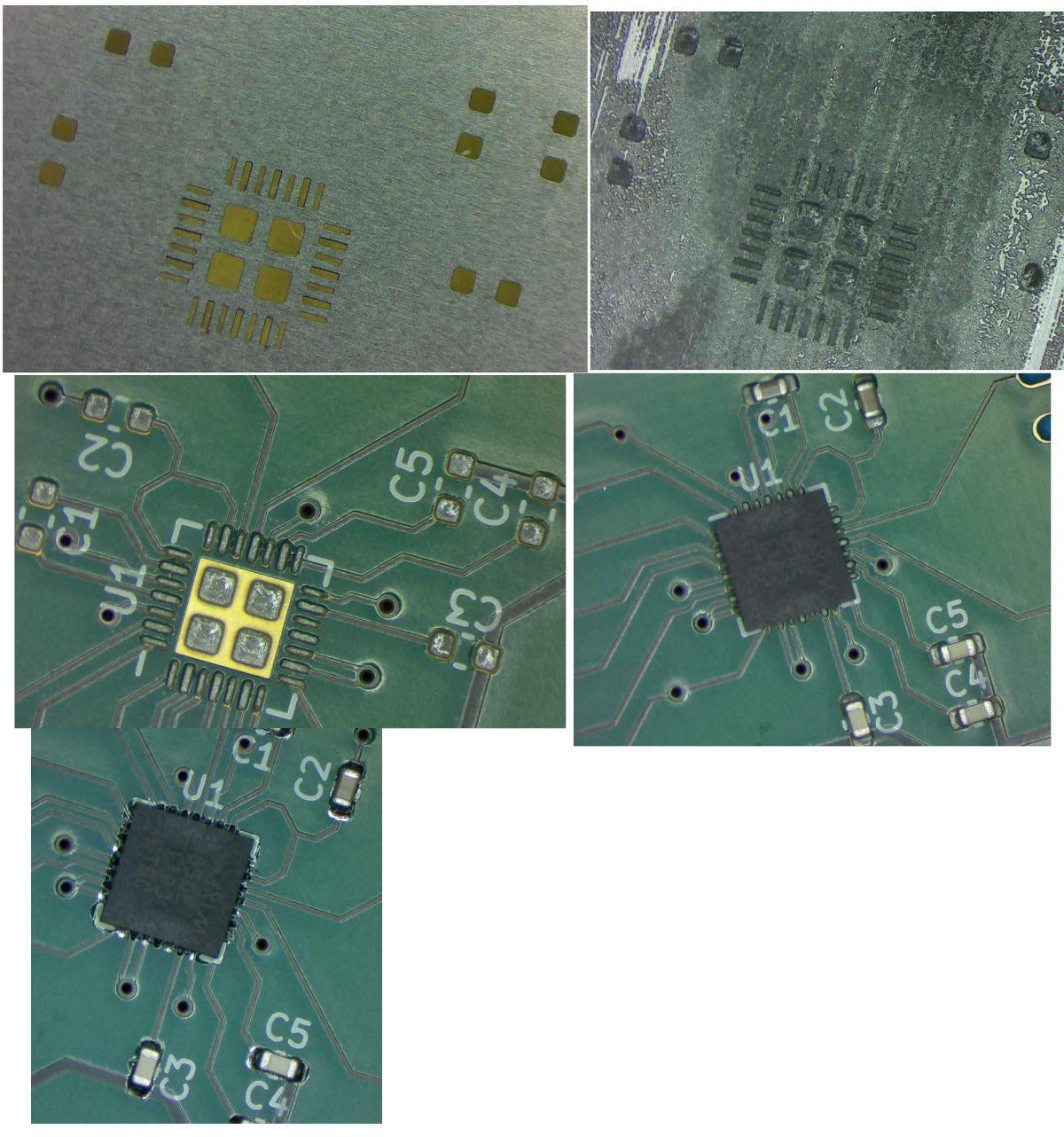 Stencil alignment, stencil with paste, paste alignment, component placement
and post solder result.
Stencil alignment, stencil with paste, paste alignment, component placement
and post solder result.
Bring up
After skimming through the MAX9850 datasheet it does seem that setting up a working audio flow will require writing a fair amount of I2C configuration registers. Ideally you would want some simple kind of test that can be used immediately after assembly to verify that the part has not been totally destroyed in the process. Needless to say you want this test to be dead simple so that you are not led to believe that the part is broken after assembly just because you made a mistake in the test code.
The MAX9850 does have a (single) GPIO pin that is controllable by a I2C register. The pin has also been routed back to the FPGA so the dead simple first test we are looking for could be to write the appropriate I2C control register to toggle this GPIO and then have the FPGA forward the signal to a LED.
Using the simple test bench I have been able to verify that both of the boards assembled so far accept I2C access and can toggle their GPIO pins.
Next up is to configure all required control registers and start streaming digital audio. Using the slightly more advanced test bench the device is configured to use a sample rate of 48.8kHz and sawtooth waveforms at two different frequencies are generated in the FPGA (one for each channel). Pressing a button swaps the sawtooth frequencies. Both assembled boards pass this test.
And finally just for fun, here is a quick integration with the MyC64 project playing the classic Bubble Bobble tune. Using branches myc64/max9850 and usbdev/max9850.
./myc64-keyb ../../../c64-psid/MUSICIANS/C/Clarke_Peter/Bubble_Bobble.prg
This does not sound quite right though, frequency (of the MyC64 design) is expected to be off but I suspect there is more to it than that. Need to examine closer at some point but for now this is good enough.