Commodore 64 experiments part-3 (FPGA)
I figured the natural next step of our MyC64 journey would be to get the emulator running on a FPGA, or more specifically the ULX3S board. Doing so requires a few support systems such as keyboard input and visual output to be in place so let us use this post to look at how that can be accomplished.
Keyboard input and control
As we already know the real C64 keyboard is a 8x8 matrix connected directly to
the CIA1 and scanned by the KERNAL code. Any modern keyboard we might find is
based on scan-codes so some conversion layer (much like what we already do in
myc64-sim) will be necessary.
In addition to keyboard input .prg injection also needs to be handled.
A straight forward way to deal with these requirements is to treat the emulator as a USB device and develop some kind of software on the host workstation that performs the keyboard forwarding and program injection. Additional control signaling such as reset/reboot could also be handled this way.
Following this approach would put good use to my USB device implementation detailed in previous posts as well as serving as motivation for thoroughly finalizing it and working out remaining bugs.
So let’s do that! We simply grab the entire USB device subsystem from github including controlling RISC-V CPU with ROM and RAM.
On the workstation software side we need to develop a program that communicates with the USB device while maintaining a workable GUI. For the USB communication we use libusb and for GUI we relay on GTK. Combining these two essentially boils down to using the asynchronous API of libusb and plugging it in to the single event loop handled by GTK.
To be more precise libusb is queried for its (Unix) event file descriptors and the GTK event loop is setup to watch these (presumably using the select system call internally). Details are found in sw/myc64-keyb.cpp.
Video output
Displaying C64 video output in a reasonable way is rather tricky as we need to comply with both the internal timing of the VIC-II (to avoid compatibility issues with existing software) as well as the timing of the chosen video format for a modern display.
Apparently this is not impossible as the Ultimate 64 manages to tweak the video timing of 576p50 to match its VIC-II output (described here). Details on the 576p50 video mode can be found here.
For this project we choose to go a different route and store intermediate VIC-II video frames in external SDRAM and display them in 640x480@60Hz over DVI/HDMI.
Audio output
Not much to say about this. The ULX3S features a 4-bit resistor ladder for DAC and we simply connect the SID’s mono output to it. Actually depending on the content 4-bit resolution does not sounds as bad as one would think. Just listen to this comparison video.
The MyC64 SoC
Combining these systems in a SoC turns out as follows

As can be seen this involves interaction between several clock domains. Especially the visual path, which is rather intense in terms of pixel shoveling, uses asynchronous FIFOs when crossing in and out of the SDRAM’s 125MHz clock domain.
The ECP5-12F only has two PLLs so we are limited in the number of clock frequencies that we can synthesize. Two blocks have strict requirements on the clock frequency. The USB block needs a clock that is a multiple of 1.5MHz and the DVI/HDMI controller needs a 125MHz clock (and a derived 25MHz pixel clock). The MyC64 block needs a clock in the neighborhood of 8MHz but it does not have to be exact (especially now that it is decoupled from the display).
So given these constraints we end up with the three clock domains 15MHz, 25MHz and 125MHz seen in the diagram. The MyC64 block uses an internal clock enable to “divide” the 15MHz clock by two.
For the SDRAM the 125MHz clock appears to be a bit too tight, both on the PCB as well as inside the FPGA (builds often fail timing constraints). So with additional clocking resources it would be preferable if this clock could be lowered to say 100MHz.
Since the async FIFOs don’t provide almost full and almost empty signaling it seemed difficult to operate the SDRAM in burst mode (i.e. as the burst is pipelined so we need to stop it before the FIFO is full to avoid overrun). Adding almost full and almost empty signaling to the FIFO was deemed out of scope since asynchronous FIFOs are already notoriously complicated in that area.
One option could have been to add a normal synchronous FIFO in series to get the almost full and almost empty signaling from that FIFO. Another option could have been to adjust the SDRAM address pointers when an overrun or underrun occurs (but since timing is already tight in the SDRAM clock domain this kind of additional logic could make things worse).
While those suggestions seem possible in theory we instead chose a simpler approach of operating the SDRAM in single access mode. Since the C64 only generates 16 colors we can store these in SDRAM instead of the full RGB value. Doing so means that we get four pixels per 16-bit memory access which appears to fall well within the time budget when operating the SDRAM at 125MHz.
The components used are gathered from various places
- SDRAM controller - Slightly modified version of the one from fpga4fun.com.
- DVI/HDMI controller - From Project Trellis DVI.
- Asynchronous FIFO - From here. This is a variant of Cliff Cummings design formally verified by Dan Gisselquist. In fact it is the subject of a Crossing clock domains with an Asynchronous FIFO article by Dan.
- MyC64-SubSys - That is what we are working on here.
- UsbDev-SubSys - That is what I was working on before this project.
Verilator simulation for the SoC
The simulator needed to be extended a bit to handle all the different components with their associated clock domains. Regrettably I dragged my feet on this and as a result wasted valuable time trying to diagnose what turned out to be rather trivial problems while running on the FPGA.
Mostly it is about handling of multiple clock domains in Verilator. Turns out that Dan Gisselquist has an excellent article titled Handling multiple clocks with Verilator so I went ahead and did something similar.
To avoid breaking the video chain we also need to simulate the external SDRAM so I added a very basic SDRAM model to rtl/myc64-soc/myc64-soc-top.v.
With all this additional stuff in place simulation with myc64-soc-sim is a
much slower than with our previous myc64-sim. So much slower that interactive
input and display does not make sense any more. Instead the SoC simulator
stores each video frame directly to the file system in PNG format.
We store video frames directly after the VIC-II output as well as the intermediate VGA frames that are being fed into the DVI controller. That is we store output both before and after the error prone SDRAM part.
The SoC simulator myc64-soc-sim is implemented in
sim/myc64-soc-sim.cpp.
Synthesis
Synthesis for my ULX3S’s ECP5-12F FPGA yields the following utilization which I find rather low given the amount of stuff we have put in. Of course we have used up all the PLLs and almost all of the block RAM but in terms of logic slices it is not that high.
Info: Device utilisation:
Info:          TRELLIS_SLICE:  6136/12144    50%
Info:             TRELLIS_IO:   128/  197    64%
Info:                   DCCA:     4/   56     7%
Info:                 DP16KD:    49/   56    87%
Info:             MULT18X18D:     3/   28    10%
Info:                 ALU54B:     0/   14     0%
Info:                EHXPLLL:     2/    2   100%
Info:                EXTREFB:     0/    1     0%
Info:                   DCUA:     0/    1     0%
Info:              PCSCLKDIV:     0/    2     0%
Info:                IOLOGIC:     0/  128     0%
Info:               SIOLOGIC:     8/   69    11%
Info:                    GSR:     0/    1     0%
Info:                  JTAGG:     0/    1     0%
Info:                   OSCG:     0/    1     0%
Info:                  SEDGA:     0/    1     0%
Info:                    DTR:     0/    1     0%
Info:                USRMCLK:     0/    1     0%
Info:                CLKDIVF:     0/    4     0%
Info:              ECLKSYNCB:     0/   10     0%
Info:                DLLDELD:     0/    8     0%
Info:                 DDRDLL:     0/    4     0%
Info:                DQSBUFM:     0/    8     0%
Info:        TRELLIS_ECLKBUF:     0/    8     0%
Info:           ECLKBRIDGECS:     0/    2     0%
As earlier mentioned, the 125MHz clock domain appears to be operating at its limits as we often get timing constraint violations after small (even unrelated) modifications to the design.
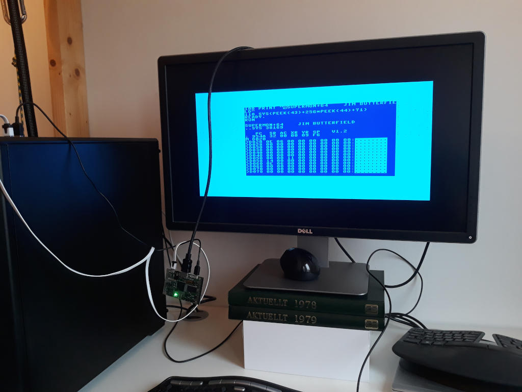
Demonstration
After loading the design on the ULX3S board and plugging in the secondary USB
connector we should expect to see the following in dmesg
usb 1-5: new low-speed USB device number 6 using xhci_hcd
usb 1-5: New USB device found, idVendor=abc0, idProduct=0064, bcdDevice= 1.00
usb 1-5: New USB device strings: Mfr=1, Product=2, SerialNumber=3
usb 1-5: Product: MyC64 - FPGA based Commodore 64 emulator as a USB device
usb 1-5: Manufacturer: Markus Lavin (https://www.zzzconsulting.se/)
usb 1-5: SerialNumber: 0123456789abcdef
At this point the device should be generating DVI/HDMI output and it is
advisable to connect a screen to verify. If all looks good we can go ahead and
connect with myc64-keyb and start typing in some BASIC commands. Any key
press (and release) that goes into the application window will be forwarded to
the USB connected MyC64 emulator.
The myc64-keyb program takes an optional argument that specifies a .prg
file to inject into emulator memory.
An interesting program to try out is the machine language monitor SuperMon by Jim Butterfield. SuperMon is the monitor used in Jim’s classic book Machine Language for the Commodore. To get hold of SuperMon itself in modern times simply go to Supermon+64 V1.2. There one can also find a video demonstrating its capabilities.
Known issues / Bugs
- USB device loses sync (and host aborts after tree packets with no response) so longer transfers often fail. Works with retry though.
- “Static noise” moves past the screen occasionally (seems to be dependent on when reset is released). Believed to be limitations of SDRAM (traces on PCB) operating at 125MHz.
- Sometimes the
.prgappears to get corrupted when loaded over USB.