Sigrok and thoughts on building a USB device
Last summer I bought a DSLogic Plus USB-based Logic Analyzer, about 6 months ago I tried it for the first time and today I hope to finish this post describing the experience. The thing comes with its own analyzer software running on the PC called DSView, but I never bothered trying that and instead went with the better known sigrok (of which DSView is a derivative).
Setting up sigrok for the DSLogic Plus
Building from source seemed rather complicated with many dependencies to be met, but luckily they also provide self contained AppImage binaries for download here. So I picked up a PulseView and a sigrok-cli binary.
Although being self contained two additional steps were required to get things going.
First setting up udev rules
git clone git://sigrok.org/libsigrok
cp libsigrok/contrib/*.rules /etc/udev/rules.d/
and second, due to legal reasons, the self contained sigrok binaries do not contain the necessary firmware for the DSLogic Plus so we need to grab a script that fetches those separately
git clone git://sigrok.org/sigrok-util
sudo sigrok-util/firmware/dreamsourcelab-dslogic/sigrok-fwextract-dreamsourcelab-dslogic
Test capture
Attaching to the USB D+ and D- of a STM32 based thumb device and capturing the signaling that occurs when the device is connected to the bus.
For background on USB 2.0 the spec summary USB in a NutShell is a highly recommended read, the similar summary USB Made Simple also provides very valuable information. For all the gory details the full specification is available here.
Sigrok provides a very neat protocol decoder for USB (as well as for many other protocols).
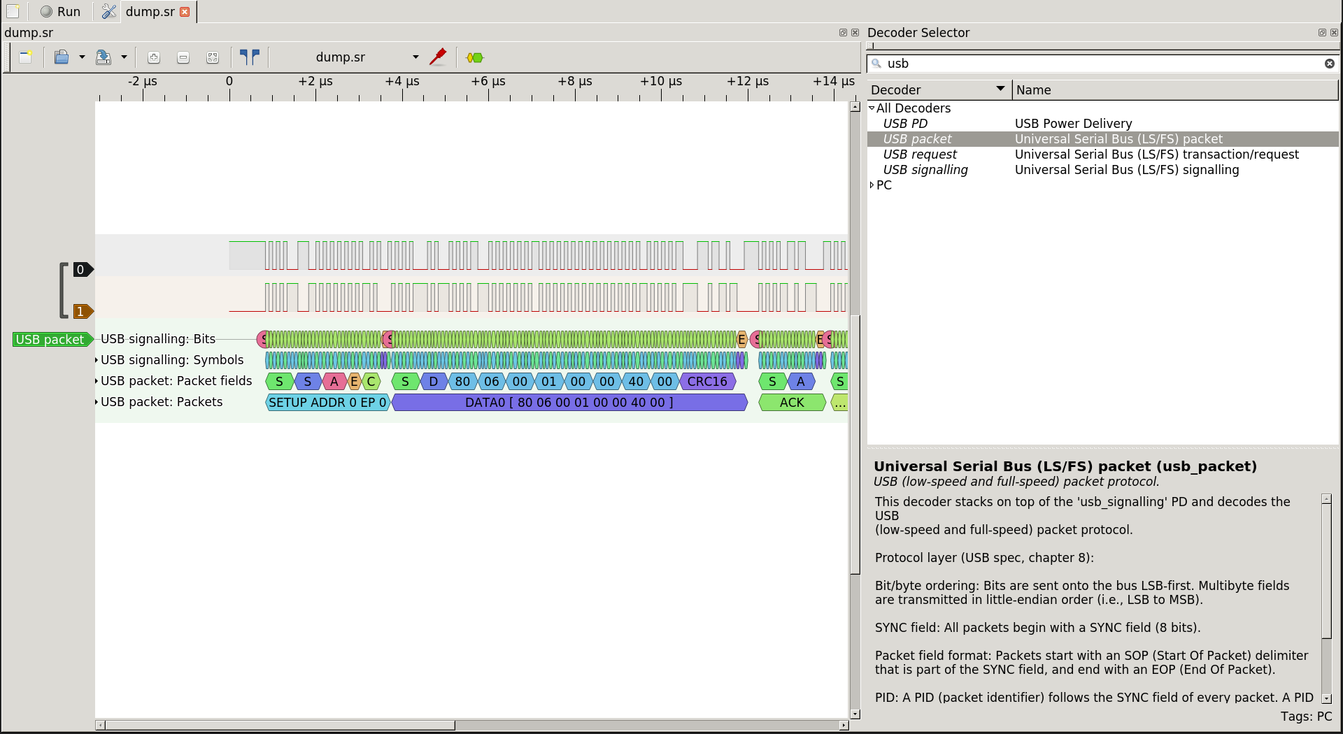
It is interesting to observe what happens when a new device is connected
# Newly connected device has address 0.
host   : SETUP ADDR 0 EP 0
host   : DATA0 [ 80 06 00 01 00 00 40 00 ]
device : ACK
host   : IN ADDR 0 EP 0
device : NAK
host   : IN ADDR 0 EP 0
device : DATA1 [ 12 01 00 02 02 02 00 40 83 04 40 57 00 02 01 02 03 01 ]
host   : ACK

host   : OUT ADDR 0 EP 0
host   : DATA1 [ ]
device : NAK
host   : OUT ADDR 0 EP 0
host   : DATA1 [ ]
device : ACK

host: <RESET for 50ms>

# SET_ADDRESS (=0x05) to 10 (=0x0A)
host   : SETUP ADDR 0 EP 0
host   : DATA0 [ 00 05 0A 00 00 00 00 00 ]
device : ACK
host   : IN ADDR 0 EP 0
device : NAK
host   : IN ADDR 0 EP 0
device : DATA1 [ ]
device : ACK

# From this point on the device has address 10.

host   : SETUP ADDR 10 EP 0
host   : DATA0 [ 80 06 00 01 00 00 12 00 ]
device : ACK
...
what appears to be going on here is that the host begins by reading the device descriptor containing, among other things, the highest USB version this device supports, idVendor and idProduct. If these are satisfactory the host goes ahead and drives a long reset followed by assigning the device a new address.
A simple lsusb confirms that idVendor and idProduct appear in the
response message retrieved before the reset.
Bus 001 Device 010: ID 0483:5740 STMicroelectronics STM32F407
Thoughts on building a USB device
If you are so inclined you might now wonder what kind of digital circuitry it would take to build a USB device. Common sense says this would be a rather significant undertaking so it seems wise to begin with some preparatory considerations.
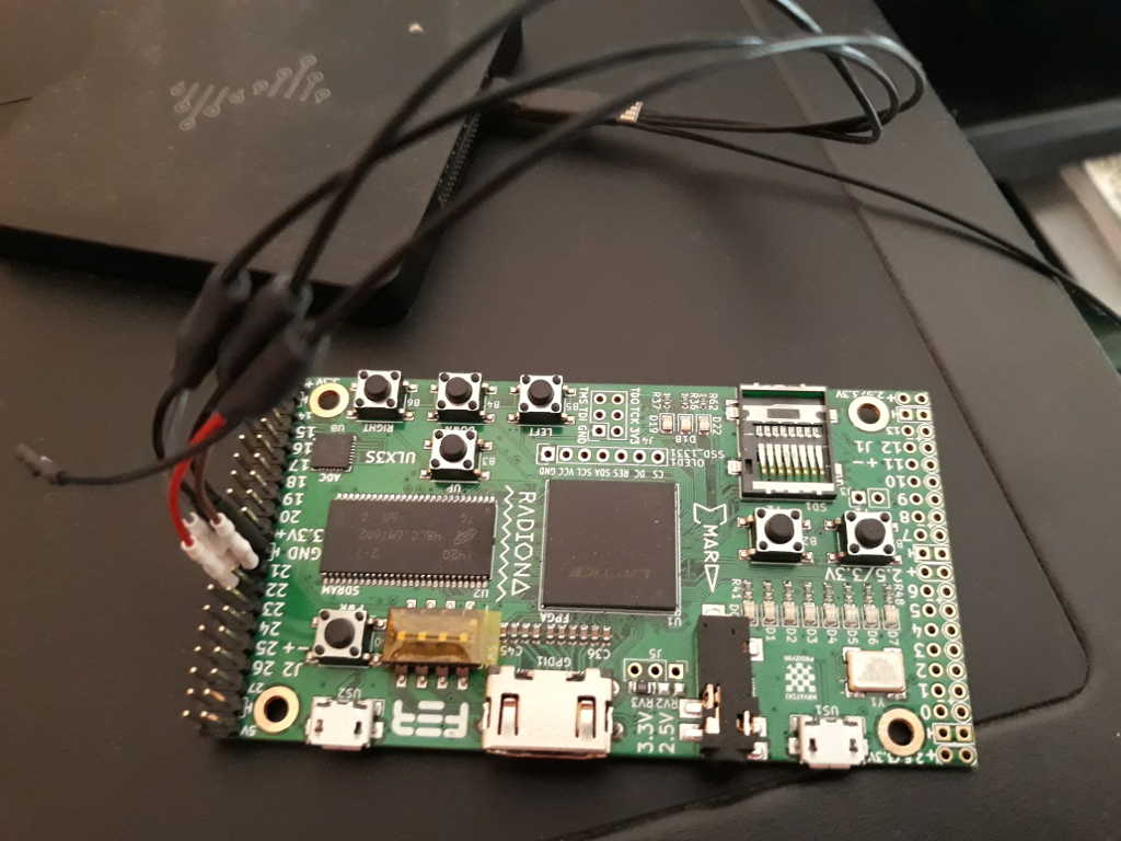
ULX3S setup
As usual the platform for my experiment will be the excellent ULX3S. The board has two USB micro female connectors where the second (designated US2) is wired directly to the ECP5 FPGA.
Schematics
Full schematics are found here but for the sake of this discussion I have extracted the relevant parts.
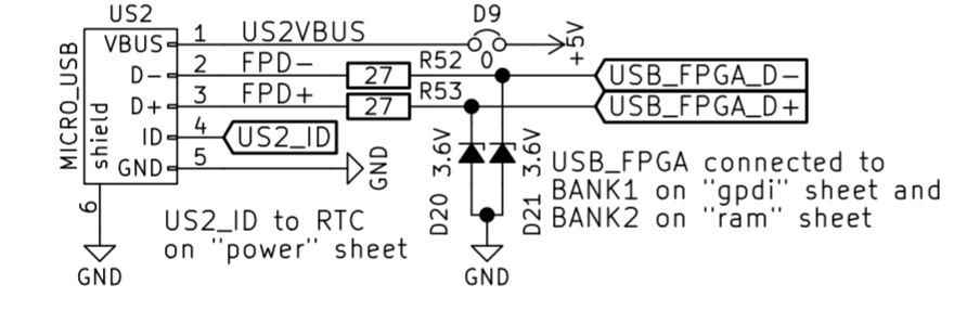
What is interesting to note here is that the USB_FPGA_D+ and USB_FPGA_D- pair is connected to the FPGA twice. One pair is connected to a differential IO cell and the second pair is connected to single ended IO cells. Reason is that USB requires us to both drive and sample differential as well as single ended. Still weird though as ECP5 docs kind of suggest that all of that could be done within one IO cell (pair).
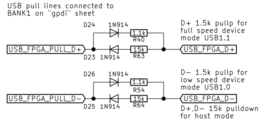
The second interesting part is that the board has FPGA controllable pull-ups. This allows us to attach/detach from the USB without physically touching any cables. As well as choosing if we want to identify as a full-speed or low-speed device.
Clocking
USB full-speed is 12Mbit/s and USB low-speed is 1.5Mbit/s, the ULX3S board has a 25Mhz crystal oscillator.
For full-speed if we were to sample at exactly the right spot a 12Mhz clock should suffice, but in reality this is not possible (without phase adjusting the clock). So instead one typically settles for oversampling with a factor of four (so a 48Mhz clock would be needed).
Now a 25Mhz clock does not directly PLL into a 48Mhz clock (nor any other reasonable multiple of 12Mhz). It does however PLL it into a 15Mhz clock that can be used for low-speed (oversampling with a factor 10).
Eventually though for full-speed we can use two PLLs in cascade configured as follows to reach exactly 48Mhz.
markus@workstation:~$ ecppll -i 25 -o 60
Pll parameters:
Refclk divisor: 5
Feedback divisor: 12
clkout0 divisor: 10
clkout0 frequency: 60 MHz
VCO frequency: 600
markus@workstation:~$ ecppll -i 60 -o 48
Pll parameters:
Refclk divisor: 5
Feedback divisor: 4
clkout0 divisor: 12
clkout0 frequency: 48 MHz
VCO frequency: 576
Connecting the Logic Analyzer
A sturdy attachment point for the analyzer is desirable as it is rather annoying having test hook clips constantly falling off the board as soon as it is moved/touched only the slightest.
Luckily since it is a FPGA we can route the USB_FPGA_D+ and USB_FPGA_D- pair “out on the other side” to make it available on the pin header. This is mechanically stable and has the additional advantage of being isolated from the actual signals so there is no risk of interference from the analyzer probes.
Sigrok support
Having powerful tools such as the Sigrok suite and the Logic Analyzer will prove invaluable for the task ahead. In fact, as we shall soon see, they will be useful in not only the obvious way.
Capture signaling/traffic between the USB host and FPGA would be the obvious application and while this will eventually be its main use we need to get quite a lot of things working to reach that point.
In the meantime we can capture authentic host signaling and feed into RTL simulation. Doing so can be easily accomplished with
sigrok-cli --input-file capture.sr -O csv | awk 'BEGIN{FS=","}{print $2$3}' - > capture.vh
and initializing the Verilog array with $readmemb.
However this presents an issue with mismatch in sampling rate. The closest the analyzer can come to 48Mhz is 50Mhz so this will be an issue for the USB device’s clock recovery.
To avoid the sampling rate mismatch another option is to have sigrok run the low level usb-signalling decoder to reliably extract the J, K, SE0 and SE1 symbols for us. To do this we use the follow python snippet to translate
#!/usr/bin/env python
import sys
import re

pattern_j = re.compile("^usb_signalling-1: J$")
pattern_k = re.compile("^usb_signalling-1: K$")
pattern_se0 = re.compile("^usb_signalling-1: SE0$")
pattern_se1 = re.compile("^usb_signalling-1: SE1$")

for line in sys.stdin:
  if (pattern_j.match(line)):
    print('01')
  elif (pattern_k.match(line)):
    print('10')
  elif (pattern_se0.match(line)):
    print('00')
  elif (pattern_se1.match(line)):
    print('11')
and then run the entire chain
sigrok-cli -i capture.sr -P usb_signalling:dp=1:dm=0 | ./usb_signalling2vh.py > capture.vh
Once our RTL simulation generates USB signaling we can feed that into sigrok for decode and verification. It is just a matter of having simulation produce a CSV file and then
sigrok-cli -i capture.csv -I csv:samplerate=48000000 -o capture.sr
where the file capture.sr can be opened and graphically decoded in
PulseView. Pretty awesome!
Wrap up
That concludes this post. Next time we will look closer at the design of our USB device, its simulation environment and traffic generator. Questions or feedback - leave a comment below!